Skip to content

Synced from upstream — do not edit this file directly

This page is generated from CARSSCenter/Mechanical-Sensors at Strain Sensor/Capsense-pcb-integration-with-strain-sensor-instructions.md as of commit 5a13573. To change it, edit the file upstream and re-run tools/sync_docs.py. Use the "Edit this page" link above to go straight to the upstream source.

Stretchable Capacitive Strain Sensor

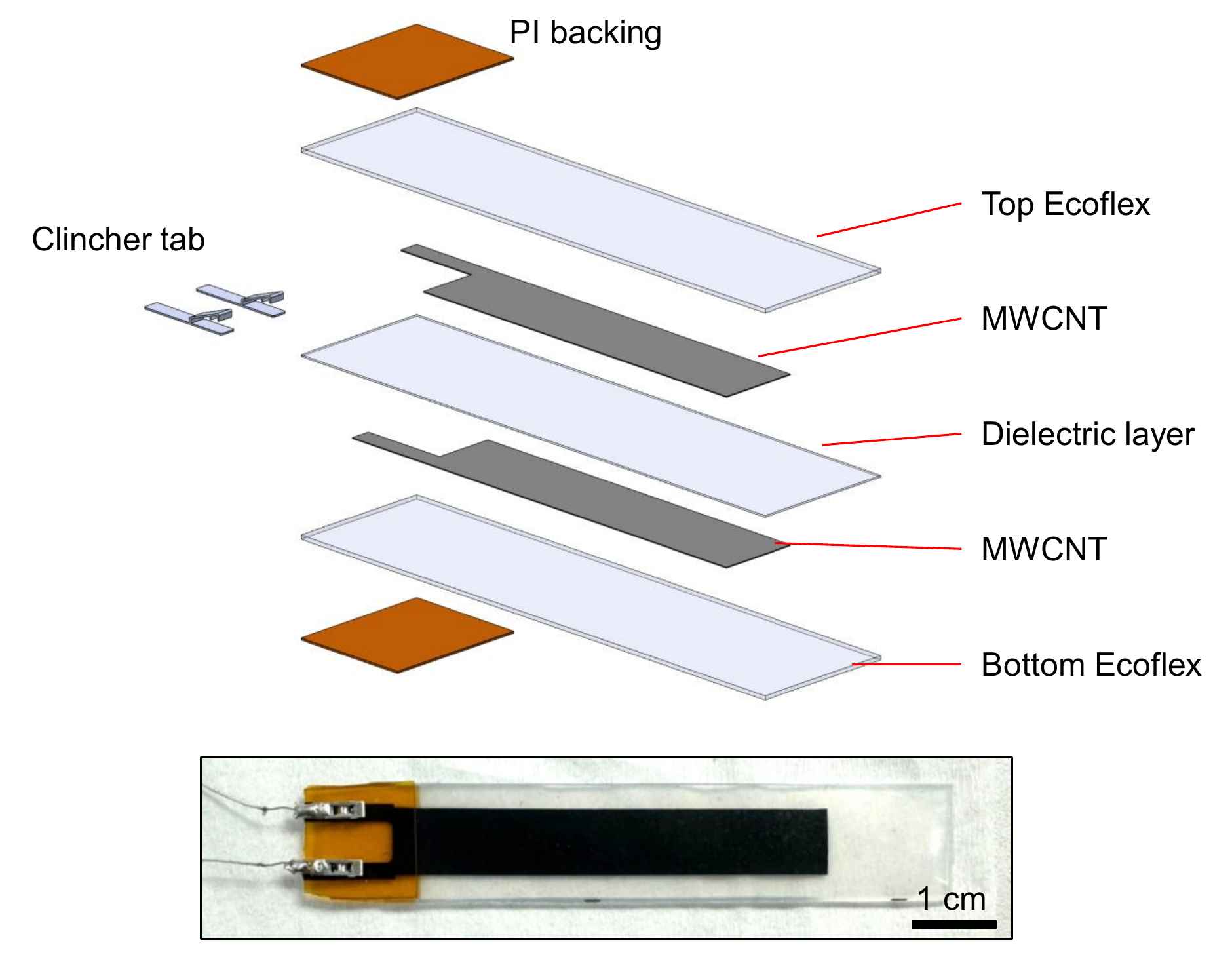
Exploded layer stack of the strain sensor (PI backing, top Ecoflex, MWCNT, dielectric layer, MWCNT, bottom Ecoflex, clincher tab) and a photo of the finished sensor with a 1 cm scale bar

Custom strain sensor: spray-coated multiwall carbon nanotubes (MWCNTs) on Ecoflex

Using Single PI Connector at the Center of the Sensor

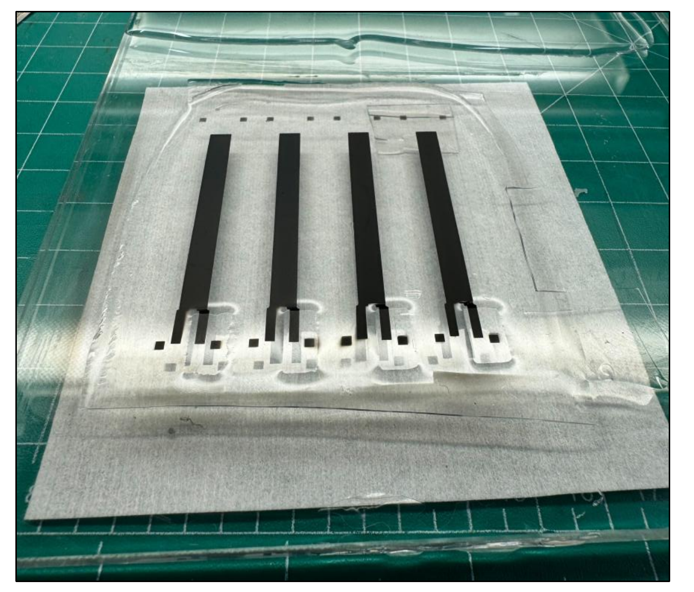
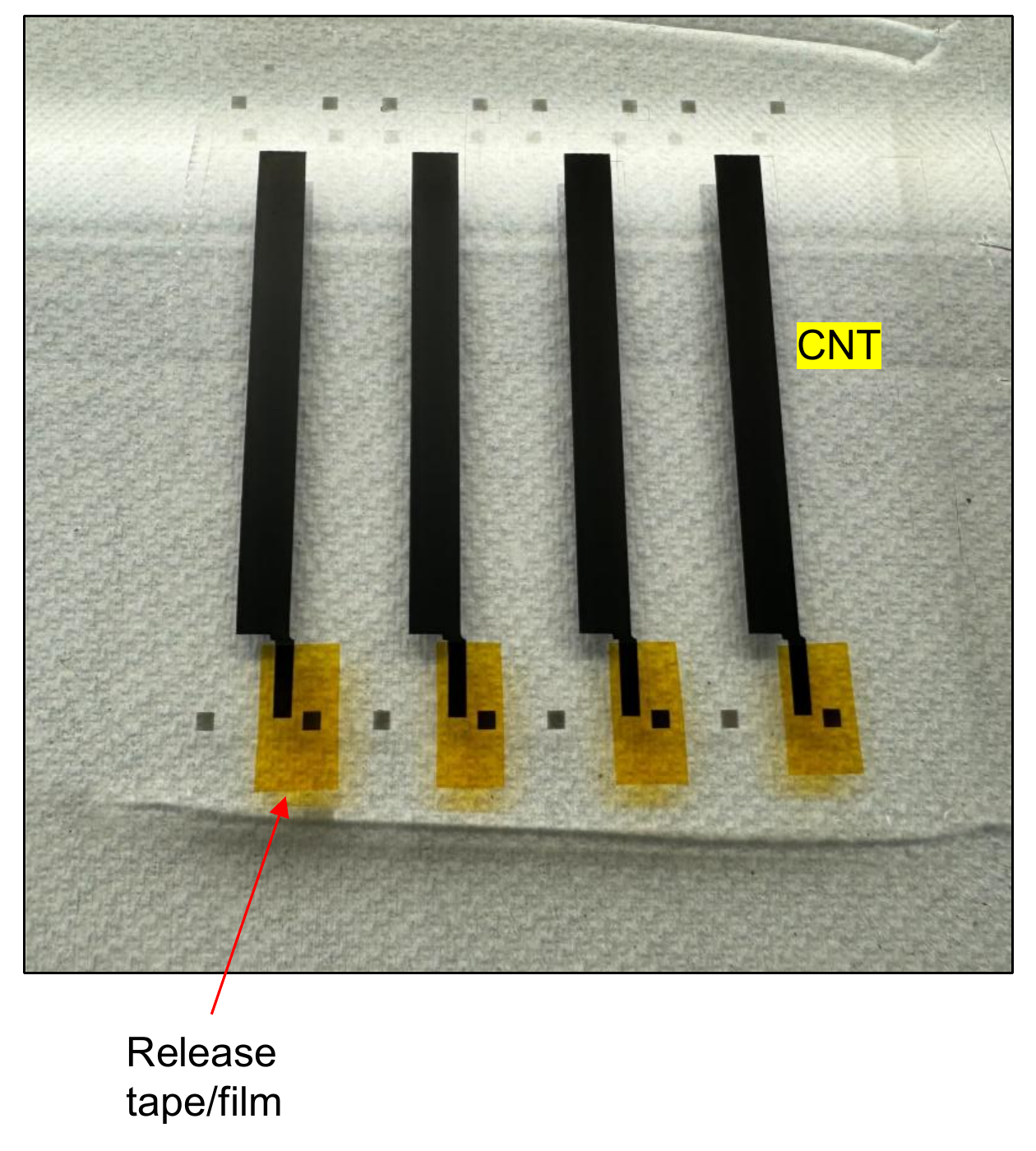
Step 1: blade coat Ecoflex on a glass substrate. Next, spray coat the first CNT layer. Then, cover the contact pad with a film or tape. After that, blade coat the middle Ecoflex layer.
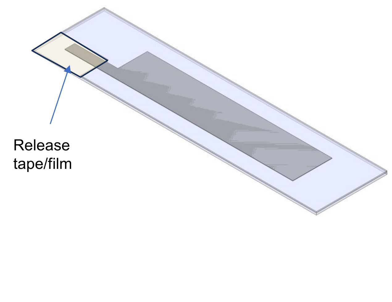
Schematic of the release tape/film placed over the contact pad before the middle Ecoflex layer is coated

Photo of four spray-coated CNT strips on fabric, with the release tape/film over each contact pad highlighted

Step 2: remove the tape to expose the contact pad. Then, spray coat the second CNT Layer.
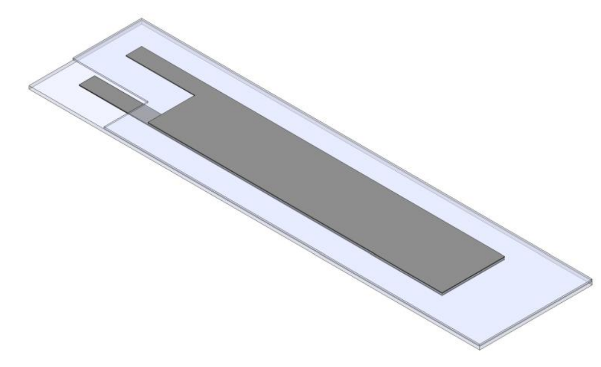
Schematic showing the contact pad exposed after removing the release tape

Photo of the sensor strips after the second CNT spray coat, laid out on a cutting mat

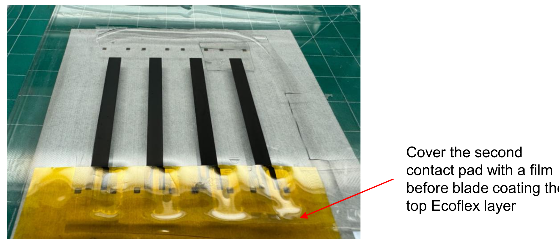
Step 3: Blade coat the top Ecoflex layer, but don't cover the exposed contact pad.
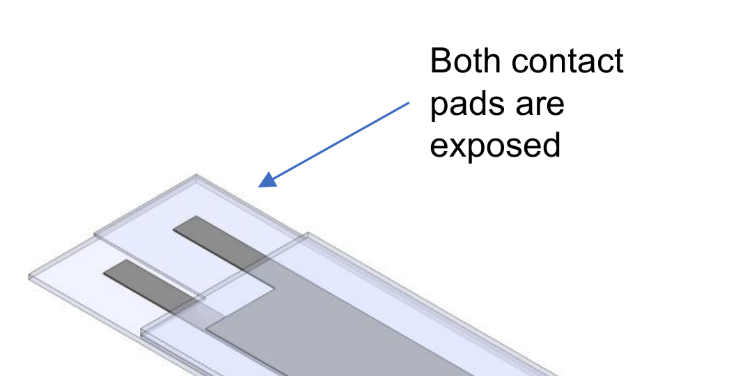
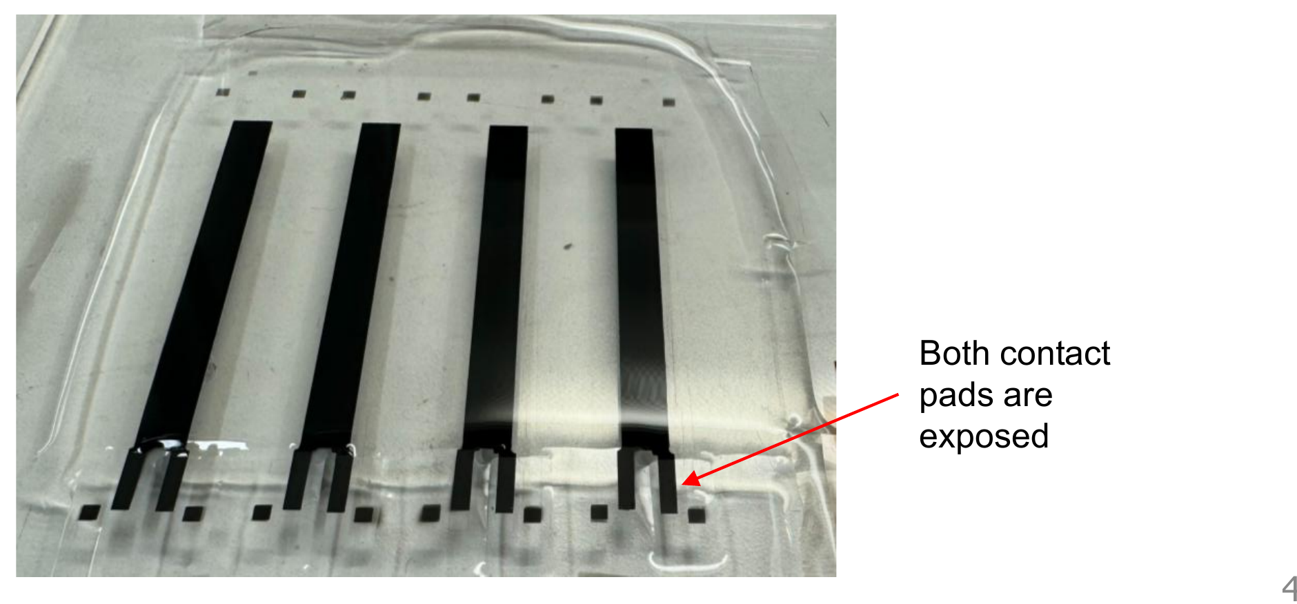
Schematic indicating that both contact pads remain exposed after the top Ecoflex coat

Photo of the sensor strips with the top Ecoflex mask in place, showing where the second contact pad should be covered with film before coating

Photo of the finished strips with both contact pads exposed after the top Ecoflex coat

Step 4: prepare a PCB or PI/electrode with the two electrodes exposed, then bond it to the two CNT contact pads using Ag paste.
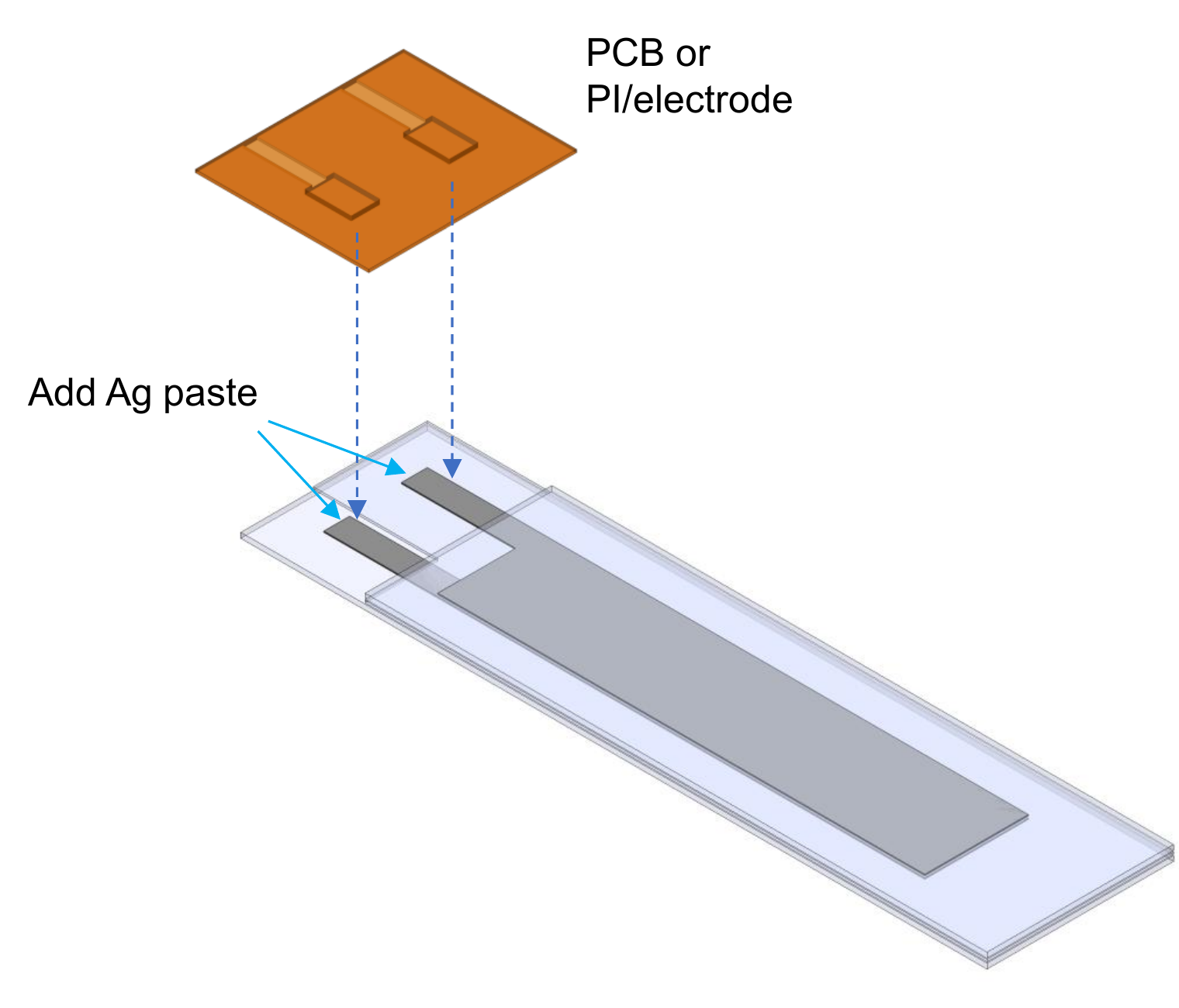
Schematic of the PCB/PI electrode being bonded to the two CNT contact pads with Ag paste

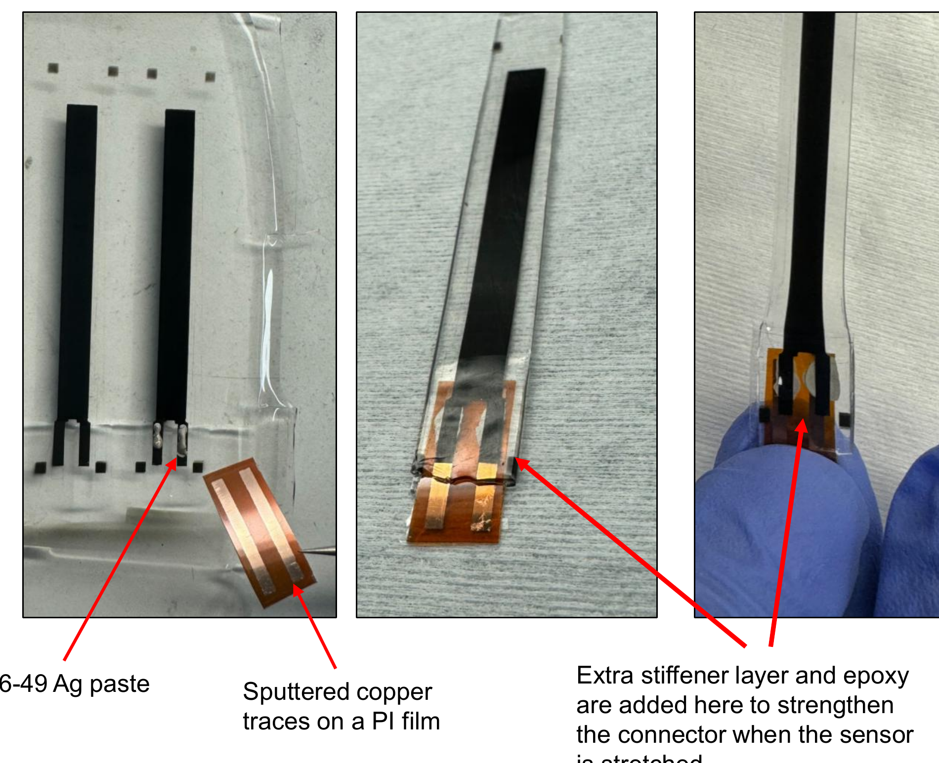
Three photos showing the 126-49 Ag paste bond, the sputtered copper traces on a PI film, and the extra stiffener layer/epoxy added to strengthen the connector when the sensor is stretched

CAD Outline and Dimensions Reference

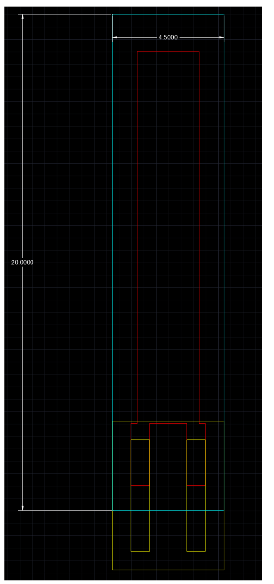
Full CAD outline of the sensor: cyan trace is the sensor contour, red trace is the CNT region, yellow trace is the PI stiffener/board, dimensioned at 20.0000 x 4.5000

  • Blue trace: sensor contour
  • Red trace: CNT region
  • Yellow trace: PI stiffener/board

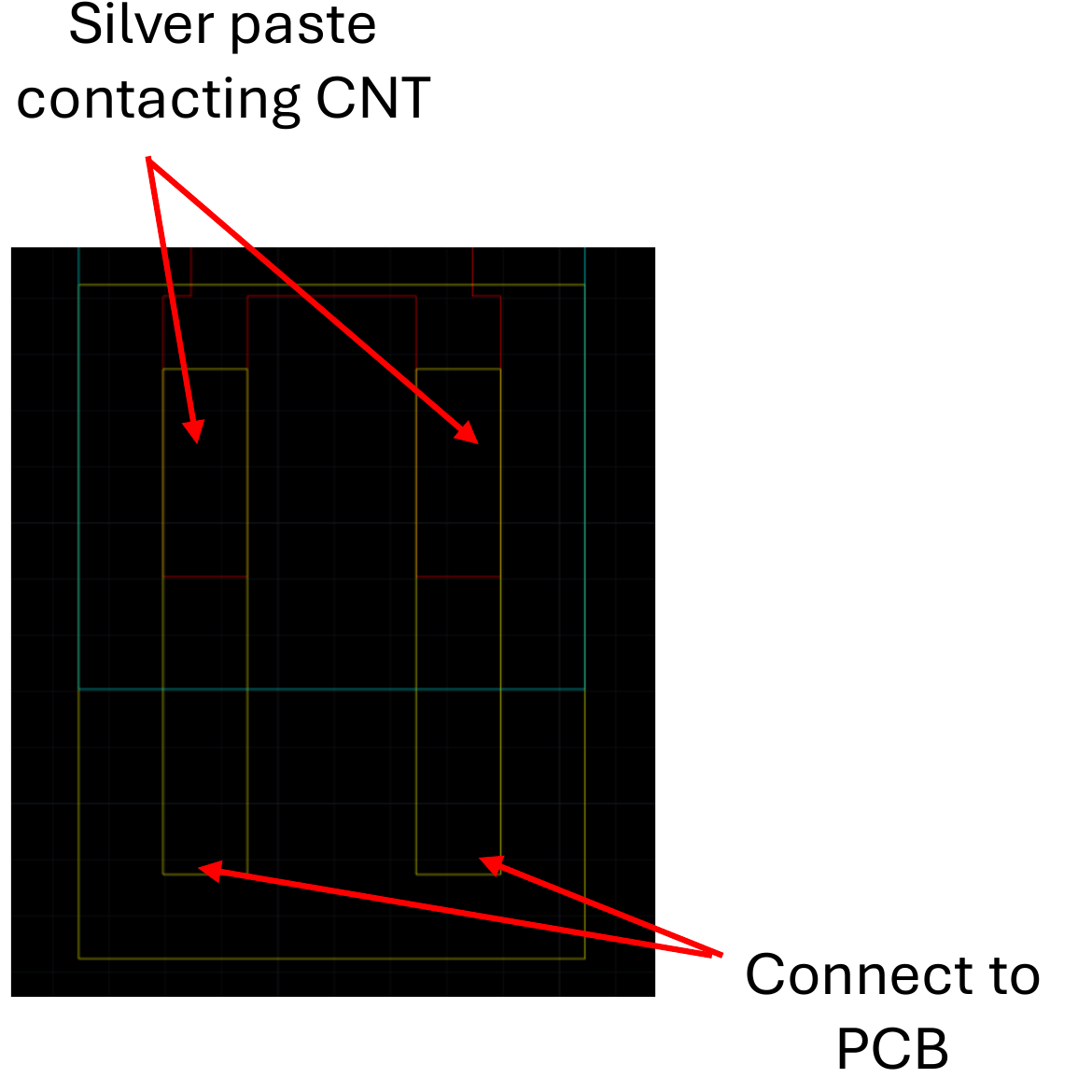
Zoomed CAD view of the two contact pads, with arrows marking where silver paste contacts the CNT and where the connector attaches to the PCB

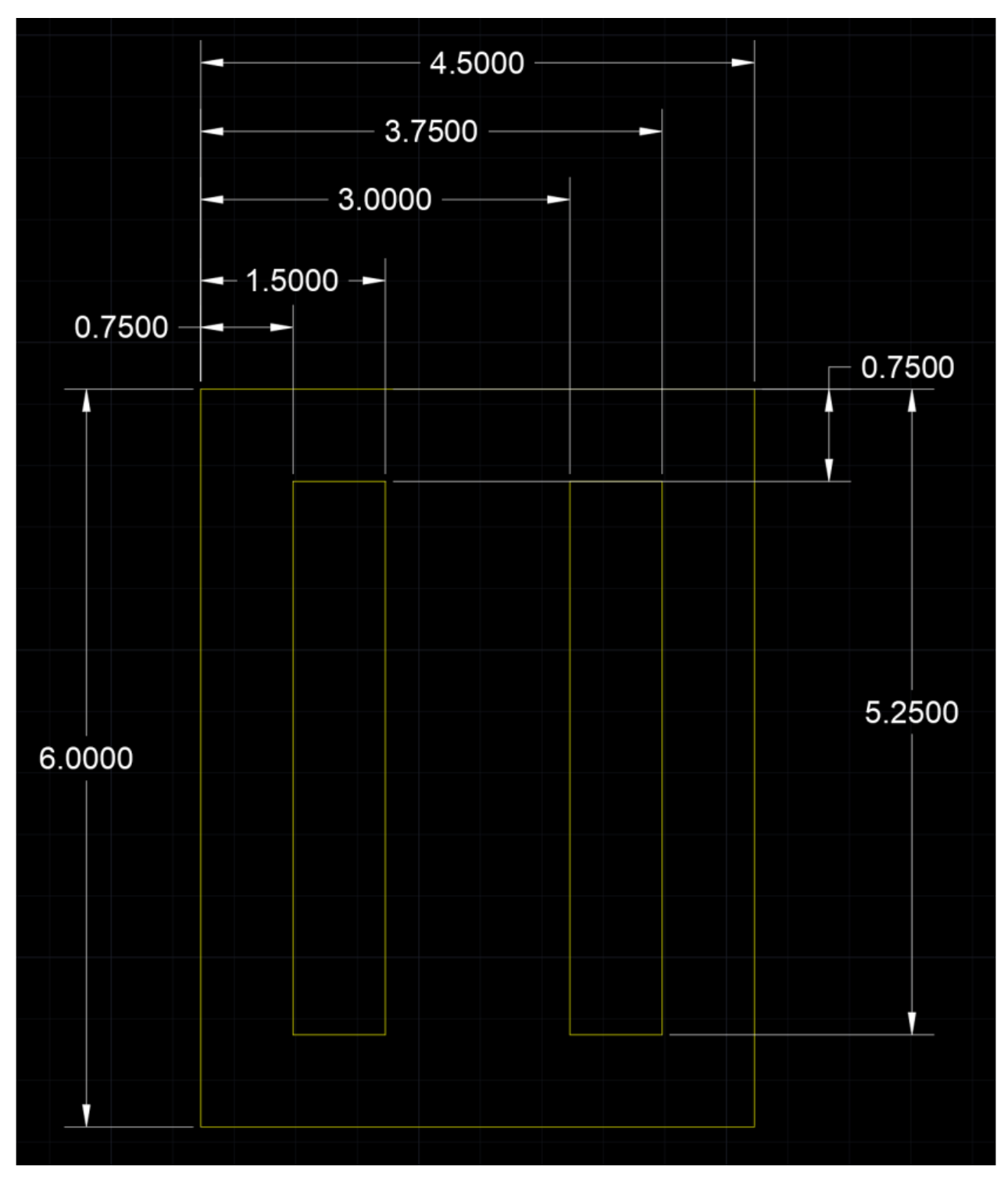
Dimensioned CAD drawing of the PI stiffener/board footprint (6.0000 x 4.5000 overall, with 0.7500-3.7500-1.5000 pad spacing)

Sensor Integrated with CapSense

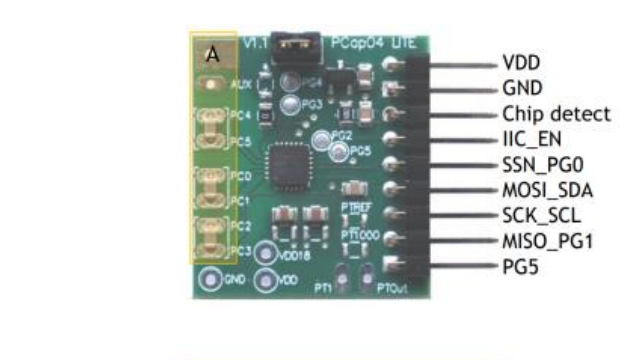
Pcap04 eval board with pin labels: VDD, GND, Chip detect, IIC_EN, SSN_PG0, MOSI_SDA, SCK_SCL, MISO_PG1, PG5

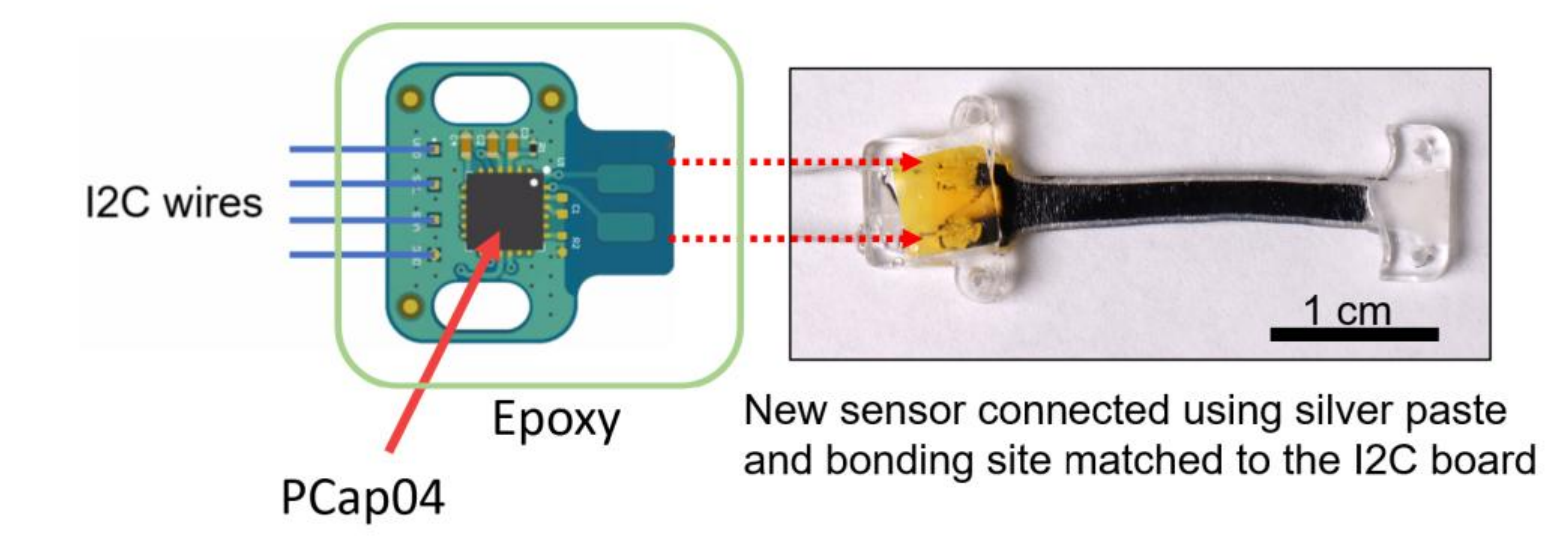
The CapSense PCB (I2C wires, PCap04 chip, epoxy strain relief) connected to the strain sensor via silver paste, with a 1 cm scale bar

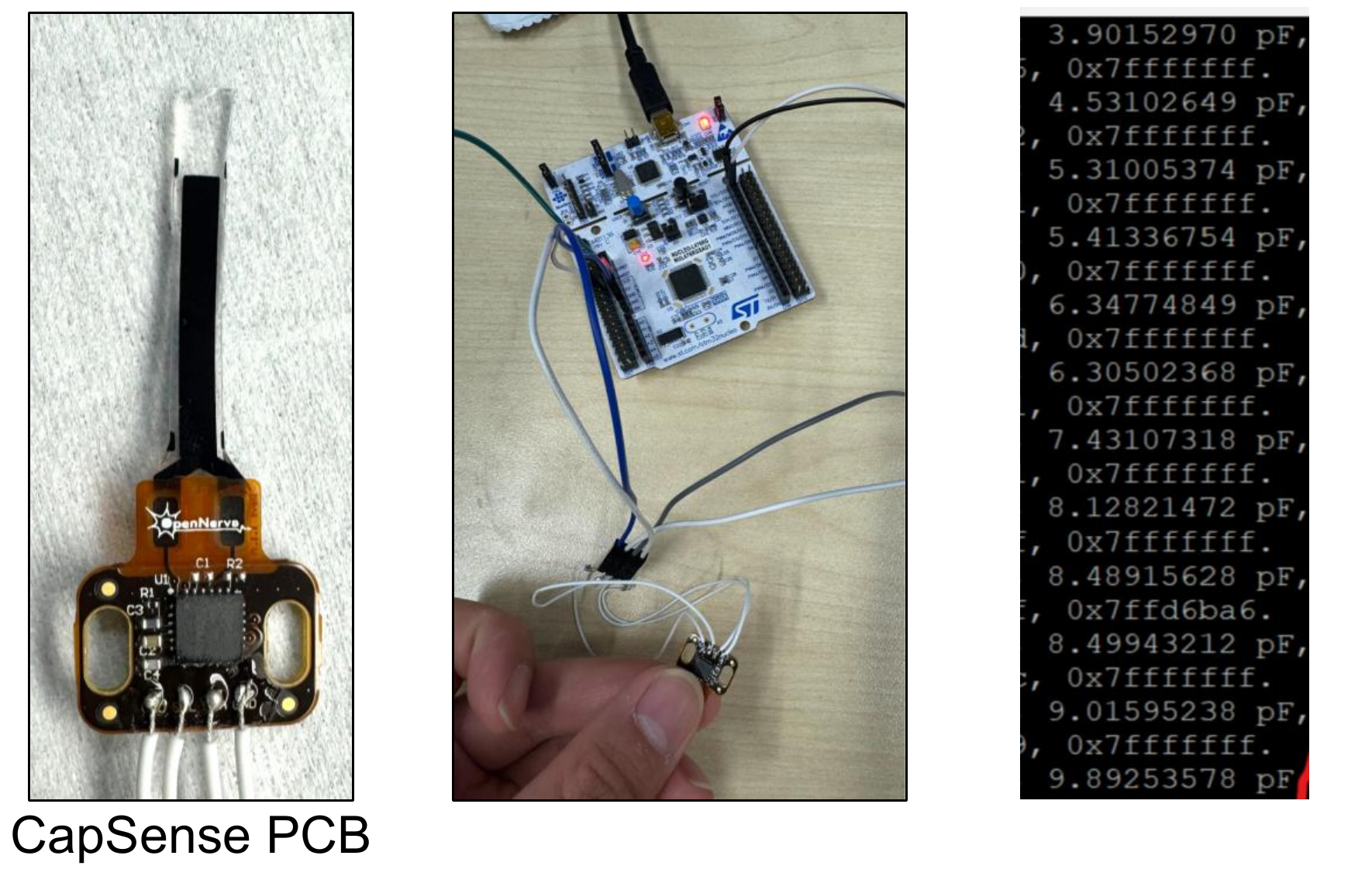
Successful reading from the evaluation board using an STM32 nucleo board via I2C.
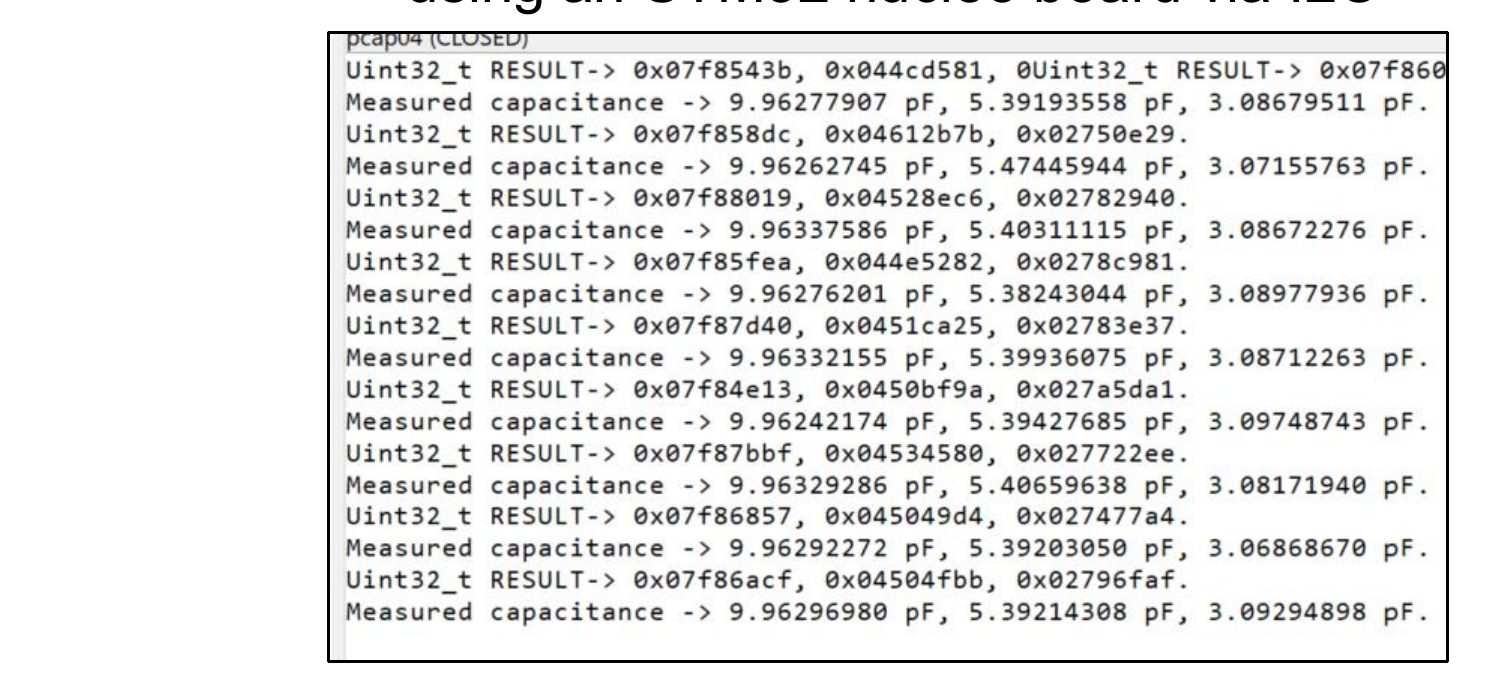
Terminal screenshot of the Pcap04 evaluation board output, showing repeated measured capacitance readings in pF

Photos of the CapSense PCB, the wired STM32 nucleo board setup, and a terminal window streaming real-time capacitance readings

Instruction:

  • Please upload the "CapMonitor_STM32_V2" code to the STM32L476RG nucleo board.
  • The Pcap04 chip on the CapSense PCB has 3 capacitance reading channels. The sensor capacitance will be recorded by the second channel. Open a serial monitor to read the real-time capacitance value.