Synced from upstream — do not edit this file directly
This page is generated from
CARSSCenter/Chemical-Sensors at fabrication-of-echem-sensors.md as of commit e5da30f.
To change it, edit the file upstream and re-run tools/sync_docs.py.
Use the "Edit this page" link above to go straight to the upstream source.
Y2-NEST5-Fabrication of Echem Sensors
Revision 1 (15 June 2024)
1. Electrode Design
The electrodes were designed using easyEDA software and were fabricated on a thin parylene C film as shown below. The electrodes are in a module that is 20 mm x 4.5 mm (20 µm thick) with conductive Pt leads (50 nm thick). The working area consists of 37 circles with 0.6 mm diameter. The counter electrode is 0.4 mm and the reference is 0.2 mm thick.
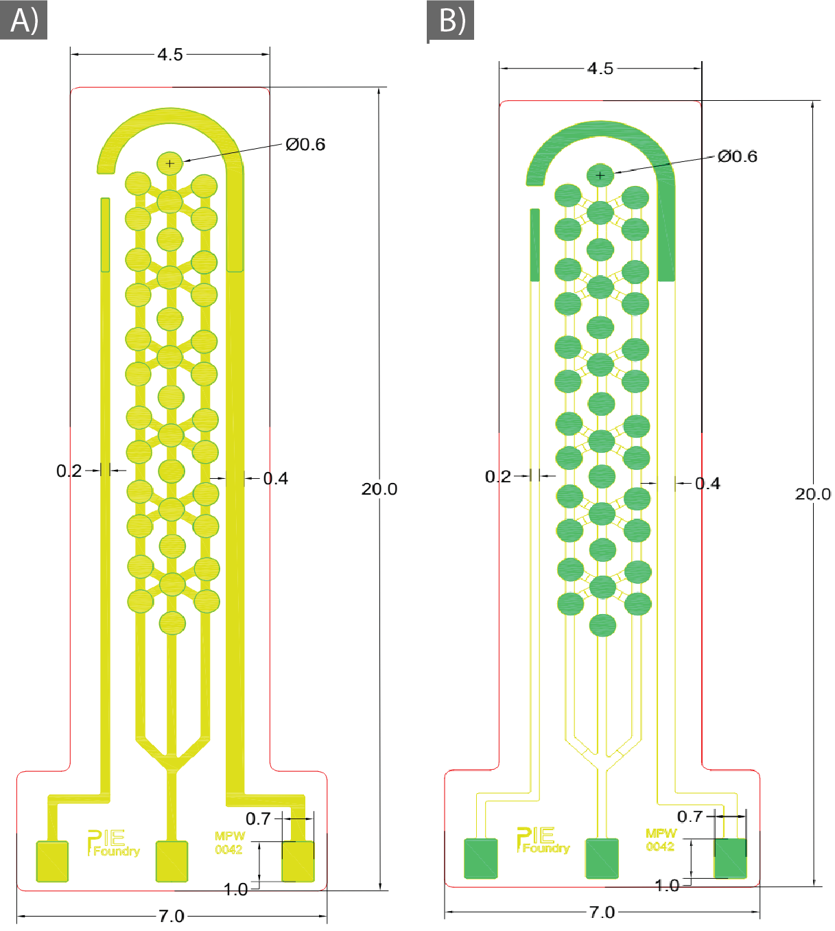
Figure 1.1. Schematic of the electrochemical sensor.
2. Parylene Electrode Fabrication
The electrodes were fabricated according to the protocol developed by Meng and Scholten, reported in the PIE foundry (https://piefoundry.usc.edu/). Below is the detailed fabrication protocol.
2.1. Base Parylene C Layer
- Wafers
- \<100> Si wafer
- 500 um thick
- 100 mm diameter
- Double-side-polished
- Dry-bake
- Dry-bake the wafers in an oven at 110 C (or higher) for at least 15 minutes;
- Or on a hotplate at a similar temperature for at least 3 minutes.
- Tool: Cascade Tek or Lindberg Blue vacuum oven
- Parylene C Deposition
- Deposit a 10 micron thick layer of Parylene C on to wafers using Parylene C deposition protocol on section 4.1.
- Thermal Anneal
- Vacuum anneal Parylene C coated wafers
- Time: 4 hour
- Temperature: 150 C
- Pressure: Full vacuum
- Tool: Cascade Tek oven
- Oxygen Plasma
- Expose wafers to oxygen plasma
- Time: 300 seconds
- Temperature: Room temperature
- Pressure: 125 mTorr
- Power: 100 W
- Flow: 30 SCCM O2
- Tool: YES Asher
2.2. Electrode Layer
- Image Reversal Lithography
- Prepare an image reversal photoresist mask of the electrodes, traces and contact pads, using the protocol on section 4.2.
- Confirm thickness of photoresist with profilometer. Target is 1.1 ± 0.1 micron.
- Oxygen Plasma
- Expose wafers to oxygen plasma
- Time: 300 seconds
- Temperature: Room temperature
- Pressure: 125 mTorr
- Power: 100 W
- Flow: 30 SCCM O2
- Tool: YES Asher
- Metal Deposition
- Ti/Pt/Au/Pt stack with thickness of 20/25/100/50 nm.
- Tool: CHA Mark 50 Evaporator
- Lift-Off
- Lift-off excess metals to define the pattern using the protocol on section 4.3.
2.3. Insulation of Parylene C Layer
- Oxygen Plasma
- Expose wafers to oxygen plasma
- Time: 300 seconds
- Temperature: Room temperature
- Pressure: 125 mTorr
- Power: 100 W
- Flow: 30 SCCM O2
- Tool: YES Asher
- Silanization
- Silanize Pt surface of metal layer prior to insulation coating using the protocol on section 4.4.
- Parylene C Deposition
- Deposit a 10 micron thick layer of Parylene C onto wafers using the Protocol on section 4.1.
- Thermal anneal
- Vacuum anneal Parylene C coated wafers
- Time: 4 hour
- Temperature: 150 C
- Pressure: Full vacuum
- Tool: Cascade Tek oven
2.4. Parylene Etch #1
- Etch Mask
- Prepare a photoresist etch mask, approx. 15 um thick, defining the outline of the MEA using the protocol on section 4.5.
- RIE Etch
- Etch approximately 10 microns of Parylene C using 𝑂₂ RIE. Etch depth should match the first Parylene C layer thickness.
- Time: Approximately 60 minutes
- Temperature: Room temperature
- Pressure: 150 mTorr
- Power: 150 W
- Flow: 50 SCCM O2
- Tool: Oxford RIE 80
- Current estimated etch rate: 0.185 micron/minute (1 wafer); 0.165 micron/minute (2 wafer)
- Strip Mask
- Strip photoresist mask in sequential baths of acetone (2-5 minutes), isopropanol (2-5 minutes), and rinse 3x in DI water.
- Blow dry with nitrogen
- Dry Bake
- Dry bake wafers under partial vacuum and nitrogen flow
- Time: > 15 minutes
- Temperature: 60 C
- Pressure: 15" Hg
- Flow: 15 SCCM nitrogen
- Tool: Cascade Tek or Lindberg Blue vacuum oven
2.4. Parylene Etch #2
- Etch Mask
- Prepare a photoresist etch mask, approx. 15 um thick, defining the outline of the MEA, and the openings over the electrodes and contact pads using the protocol on section 4.5.
-
RIE Etch
When exposing the electrodes we etched down with deep reactive ion etching (DRIE) only 90% of the way, and then removed the last ~1 micron of insulation using a pure oxygen RIE to minimize any etching of the Pt surface. - Etch approximately 10 microns of Parylene C using O2 RIE. Etch depth should match second Parylene C layer thickness. - Time: Approx. 60 minutes - Temperature: Room temperature - Pressure: 150 mTorr - Power: 150 W - Flow: 50 SCCM O2 - Tool: Oxford RIE 80 - Current estimated etch rate: 0.185 micron/minute (1 wafer); 0.165 micron/minute (2 wafer) 20. Strip Mask - Strip photoresist mask in sequential baths of acetone (2-5 minutes), isopropanol (2-5 minutes), soak in DI water 21. Release MEAs - Slowly peel MEAs off wafer while submerged in water using tweezers.
2.4. Post-Processing
- Thermal Anneal
- Vacuum anneal MEAs sandwiched between ceramic plates.
- Purge oven 3x with nitrogen prior to starting program
- Time: 48 hour; 8 hour ramp up; 8 hour ramp down
- Temperature: 200 C
- Pressure: Full vacuum
- Tool: Cascade Tek
- High-Temperature Anneal
- Install Dataplate hotplate in Cascade Tek vacuum oven using rubber feedthrough and wire terminal block.
- Seal leaks around feedthrough using Parafilm.
- Place devices sandwiched between ceramic plates on hotplate
- Set temperature to 275 with 180 C per hour ramp
- Pump down oven, then close vacuum and flood with nitrogen at 25-50 sccm
- Ramp for 1.5 hour, then bake for an additional 3 hours; Unplug the hotplate and let cool below 90 C.
- Time: 3 hour bake; 1.5 hour ramp up; 1-2 hour cool down.
- Temperature: 275 C
- Pressure: Atmosphere
- Flow: 25-30 SCCM nitrogen
- Tool: Cascade Tek oven and Dataplate hotplate
- Oxygen Plasma
- Attach MEAs to carrier wafer (Si or glass) face-up, using small bits of kapton tape.
- Time: 300 seconds
- Temperature: Room temperature
- Pressure: 125 mTorr
- Power: 100 W
- Flow: 30 SCCM O2
- Tool: YES Asher
3. Packaging
- Cut the PEEK (250 micron thickness, from McMaster) with a size more than the electrode connector side.
- Attach the connector section of the electrodes to the backing PEEK using small strips of polyimide tape.
- Permanently adhere the electrode to the PEEK using Epotek 301 epoxy.
- Mix the epoxy.
- Put two small drops on both side of the electrode to diffuse between the Parylene and PEEK
- Place the electrodes under vacuum using a bell jar to remove air bubbles
- Cure the epoxy in an oven at 55 C for 1.5 hours.
- Remove the polyimide tape
- Cut the PEEK from edges of the electrodes using an exact knife and/or microscissors.
4. Protocols
4.1. Parylene C Chemical Vapor Deposition
Warnings
Items not allowed in chamber: wood, scotch tape, liquids, anything capable of off-gassing.
- Parameters for Parylene C:
- Vaporizer heater: 175 °C (do not alter)
- Pressure set point: Base + 15 Vacuum Units (typically 35)
- Pyrolysis Heater: 690 °C
Setup (~0.5 hours)
- Determine from log approximately how much Parylene C should be used to obtain desired thickness: Most current measurements suggest 30 grams for 10 microns across 12 wafers.
- Weigh out Parylene dimer using the scale in the cleanroom.
- Fill out the log sheet. If you are doing Run 5, 10, 15, etc., check the "Parylene Machine Maintenance" document and notify superuser.
- Check cold-trap, vaporizer door, and chamber lid o-rings to make sure each is clean and will form a good seal. If necessary, clean chamber lid o-ring by peeling off with tape and use only small amounts of Micro-clean and dry immediately afterwards to prevent damage to rubber. If you replace any o-rings, check for additional spares and order if necessary (see end of protocol for vendors). Also, notify superuser.
- Do NOT remove the chamber base L-gasket unless you are having leak issues or you see Parylene pieces sticking out. Frequent removal and handling makes it crack sooner. Overtightening the c-clamp also makes it crack sooner.
- Wipe all interior surfaces of the machine (chamber, lid, rotating table, bottom plate, baffle, etc.) and the cold trap probe with Micro-90, even if it was wiped down after the last run. Do not wipe the shelf, as this leaves TexWipe fibers that get coated over time and cause an irregular surface.
- Place the flexicool cold trap probe into the coating systems cold trap.
- Place the rotating shelf onto the base.
- Cut 6 rectangular pieces of aluminum foil 8.5x4.5 inches, and place each piece in every shelf (alternating directions) to avoid holes in the back of the wafers.
- Place your wafers onto the foil lined shelves. Two 100 mm diameter wafers can fit on each shelf.
- Place a 1x3" clean, labeled glass slide on each shelf for thickness measurements.
- Make sure none of the samples extend beyond the edge of the rotating table, as overhanging samples may hit the baffle when the table rotates.
- Carefully lower the chamber around the shelf and place the chamber lid on top of the chamber.
- Dimer boat construction: Cut a rectangular piece of aluminum foil 11x4 inches, and form the aluminum piece lengthwise along the outside diameter of the boat form (metal tube). Face shiniest side of foil toward boat form. Fold in the ends of the foil, and remove the boat from the form. The dimer boat must be no more than 7.5 inches long.
- Pour Parylene C dimer pellets into the foil boat and load the boat into the vaporizer. Important: When loading the boat place it only as far into the vaporizer as necessary, do not push towards the back. Close and lock the vaporizer door.
Running Parylene C System (minimum 2 hours)
- Twist "Emergency Stop" button until it pops up.
- Push the "Main Power" button. Wait for all the controllers on the display panel to come on and display current values.
- Turn Vacuum knob to "Vacuum". Initial Vacuum reading should be around 1000. Press down on the lid for the first 20 seconds to help make a good seal. It should reach ~100 in a couple of minutes. If not, your sample is off-gassing or there is a leak in the system.
- Turn ON the chiller. Wait a minimum of 45 minutes before starting the deposition process.
-
Check that the vacuum level has reached at a level of 5 units (or lower). This may take up to 1 hour total if there are many items degassing. If the pump takes much longer there may be a leak.
Common leaks are caused by cracks or Parylene residue along the chamber O-ring or gasket, leaks along the O-ring within the chamber viewing window, leaks where the pressure sensor attaches to the tool (if replaced recently). 20. Turn on FURNACE and VAPORIZER, and press the PROCESS START/STOP button. The green button should now be illuminated. This will allow the furnace to begin heating up, however the process will not begin until pressure set points have been reached. 21. Wait for deposition.
In order for coating to begin, all the following must happen: 1) the chamber gauge must reach 135 °C, 2) the furnace must reach 690 °C, and 3) the vacuum reading must be less than 11. Then the vaporizer will begin heating, and the coating process will start. If any of the conditions are not met, something is wrong and you should contact the superuser. 22. The machine will run for several hours, depending on the coating thickness. The run will stop automatically and begin to cool down when the process is complete (green button will be blinking).
Cool Down and Cleanup (~1 hour)
- Let the system cool until the Vaporizer temperature is less than 90 °C to prevent harmful gasses from escaping.
- Turn off the chiller and wait > 5 minutes.
- Press the PROCESS START/STOP button.
- Turn the left two switches to "Disable" and the vacuum switch to "Vent."
- Push the "Emergency Stop" button down.
- Carefully remove cold-trap probe from machine and place in holder to defrost.
- Remove the chamber lid.
- Remove samples.
- Peel Parylene C from the inside surfaces: chamber, lid, rotating table, bottom plate. If Parylene film is thin (< 3 microns, rainbow sheen) leave it until clean up after the next run.
- Wipe inside surfaces with Micro-90 (except the shelf).
- If necessary, clean chamber lid o-ring by peeling off with tape and use only small amounts of Micro-clean and dry immediately afterwards to prevent damage to rubber.
- Open the vaporizer and discard the used foil boat.
- PERFORM THIS STEP IN MAIN LAB: Once the probe is defrosted, use a green scotch brite pad to scrape off Parylene C residue from the cold-trap probe (outside and bottom), wipe clean with a TexWipe and Micro-90. If it doesn't shine all over, you haven't cleaned enough yet. Any cloudiness or residue will lead to rust spots, which is good for neither the probe nor the pump.
- Put the probe back into the holder (NOT cold trap) for storage in between runs. If you incorrectly leave the probe in the cold trap, condensation build up can drip to the bottom and leave rust spots that are impossible to clean and bad for the machine.
- Thickness Measurement
- Use a new razor blade to cut a 1-2mm wide strip of Parylene off of one of the 1x3" glass slides from each shelf.
- Measure deposition thickness with profilometer and update log.
4.2. High Resolution Lift Off Lithography
Tweezers: Use Teflon coated or plastic tweezers that are new or very clean, to avoid trapping dirt/impurities under first Parylene layer.
- Drybake wafer
- The aim of this step is to improve photoresist adhesion to Parylene by removing moisture.
- Bake the wafers in a vacuum oven at approximately 60 °C, under light vacuum (~½) atm and constant N2 flow.
- To achieve this, slowly open the vacuum valve while increasing nitrogen flow. Allow wafers to bake for > 15 minutes.
- Time: > 15 minutes
- Temperature: 60 C
- Pressure: 15" Hg
- Flow: 15 SCCM nitrogen
- Tool: Cascade Tek or Lindberg Blue vacuum oven
- Mask Clean
- Safety: When handling Nanostrip or Piranha perform all steps in the 'Acid Hood'. Wear full acid PPE: Apron, Mask, and Large Green Gloves. Keep hood sash below the height of any containers used.
- Fill the glass 'Piranha Only' beaker with a shallow layer of Nanostrip, just enough to cover a glass lithography mask (~⅛"). Place on top of a hotplate set to 60 °C. Set the old hot plate to 60 C. Prepare two HDPE trays with DI while you wait for the hotplate to heat.
- Using the 'Piranha' tweezers (no teflon, no plastic), carefully place your mask (feature side up) in the mask holder and then the mask holder into the glass beaker. Wait > 10 minutes - Carefully transfer the mask into the first tray and rinse briefly. Transfer to the second bath and rinse 5x with DI water. Rinse tweezers thoroughly as well.
- Blow mask dry with N2
- Turn off the hotplate and allow Nanostrip to cool to room temperature.
- Disposal: After cooling to room temperature carefully pour nanostrip into waste bottle using glass funnel. Triple rinse beaker. Triple rinse HDPE trays.
- Photoresist spin (AZ 5214)
- Spin AZ 5214 photoresist to a thickness of ~1.2 microns
- Use at least three dummy spins
- Place the wafer in the spinner using the wafer centering tool. Deposit 2.5 mL of resist in the center of the wafer from a pre-prepared 3 mL syringe.
- Recipe: Program L
- 1st Spin Speed: 500 RPM
- 1st Spin Time: 5 seconds
- 2nd Spin Speed: 3200 RPM
- 2nd Spin Time: 40 seconds
- 2nd Spin Acceleration: 8 A.U (1088 RPM)
- Tool: Laurell Spinner WS-400/500B
- Softbake
- Bake the wafer on a hotplate for 1 minute @ 110 °C. Confirm temperature with IR gun. Typically requires setting the hot plate at 119 °C.
- Wafer should be placed in the center of the hot plate with the flat facing forward. Use a heat shield around the hot plate.
- After baking, store the wafer in black wafer storage box.
- Time: 60 seconds
- Temperature: 110 °C
- Tool: Lithography hood hotplate
- First Exposure
- Set UV lamp; clean chuck and mask holder; place mask in holder using mask holder vacuum and clips.
- Set lamp to 12.5 mW/cm^2
- Set timer to 3.5 s → 42 mJ/cm^2 (measured i-line 365 nm)
- Expose under hard contact
- No o-ring
- Exposure Dose: 42 mJ/cm^2
- Time: 3.5 s
- Intensity: 12.5 mW/cm^2
- Mode: Hard Contact
- Tool: OAI Mask Aligner Series 200
Detailed steps for hard contact without alignment: - Load mask - Turn ON mask vacuum and place set screws - Clean mask with nitrogen - Load wafer - Turn ON substrate vacuum - Clean wafer with nitrogen - Turn ON nitrogen purge - Lower mask - Raise wafer till flush with mask - Turn OFF substrate vacuum - Turn ON hard contact - Turn OFF nitrogen purge - Wait ~30 seconds; you should see clear Newton rings at the interface of the wafer and mask. - Expose - Turn ON nitrogen purge and wait ~30 seconds - Turn OFF hard contact - Turn ON substrate vacuum - Lower wafer chuck - Raise mask - Turn OFF substrate vacuum 6. Image reversal bake - Bake the wafer on a hotplate for 63 seconds @ 110 °C. Confirm temperature with IR gun. Typically requires setting the hot plate at 119 °C. - Wafer should be placed in the center of the hot plate with the flat facing forward. Use a heat shield around the hot plate. - Time: 63 seconds - Temperature: 110 °C - Tool: Lithography hood hotplate 7. Flood expose - Exposure Dose: 280 mJ/cm^2 - Time: 23.3 s - Intensity: 12.5 mW/cm^2 - Mode: Flood (no mask) - Tool: OAI Mask Aligner Series 200 8. Develop - After exposure, immediately place wafer in bath of DI water to avoid heating/reduce gas bubble formation for 2 minutes - Prepare developer bath: 1:4 ratio of AZ340 to DI H2O in a shallow plastic tray marked for developer use 40 mL of developer and 160 mL of DI H2O for 200 mL total - Place wafer in developer and apply mild agitation for 18 seconds - Quench in wafer in DI bath and rinse gently 5x - Blow wafer dry with nitrogen 9. Inspect - Check feature marks, alignment marks under microscope with yellow light filter - Check resist thickness, should be 1.1-1.3 microns
4.3. Metal Lift Off on Parylene C
PPE: Conduct lift-off only in fume hoods with sash lowered. Wafers should be lowered/raised from solvent baths using wafer dippers only. Cleanroom gloves and goggles required. Thick solvent gloves recommended.
Lift-off protocol for Pt stack:
- Prepare solvent baths
- All solvent baths should be prepared in glass beakers designated for lift-off, as the process generates metal microparticles that cannot be easily cleaned.
- Glass beaker on hotplate, set to 60 ºC, with small layer of NMP/PG remover
- Glass beaker at room temperature with small layer of NMP/PG remover
- Glass beaker at room temperature with large amount of isopropanol
- Glass beaker or HDPE tray with DI water
- Warm NMP soak
- 20-40 minute soak in warm (60 ºC) NMP. Features should begin to appear after a few minutes. If not, the photoresist profile may be incorrect.
- After 20 minutes spray with NMP from a squeeze bottle. Devices should be completely resolved before moving to next bath.
- NMP rinse
- Transfer wafer to the room temperature NMP bath.
- While holding the wafer at a downward sloping angle, spray vigorously with an NMP squeeze bottle to remove all remaining metal flakes.
- Rinse any remaining metal flakes in the NMP bath for ~5 minutes.
- IPA Rinse
- Transfer wafer to the room temperature IPA bath.
- While holding the wafer at a downward sloping angle, spray vigorously with an IPA squeeze bottle to remove all remaining metal flakes.
- Soak in IPA bath for 10 minutes
- DI Rinse
- Soak wafer in DI water bath. Rinse ~3-5x with DI water.
- Dry
- Blow dry wafer with nitrogen.
- Dry-bake wafers for > 15 minutes
- Time: > 15 minutes
- Temperature: 60 C
- Pressure: 15" Hg
- Flow: 15 SCCM nitrogen
- Tool: Cascade Tek or Lindberg Blue vacuum oven
4.4. A-174 Adhesion Promoter Treatment
Overview
Native Parylene has low adhesion to metal surfaces. Pretreating the metal surface with A-174 silane (Gamma-Methacryloxypropyltrimethoxysilane, CAS# 2530-85-0, Special Coating System, Indianapolis, IN, USA) prior to Parylene deposition can significantly increase the Parylene-metal bonding. A-174 is a liquid that needs to be mixed with IPA and DI water in a specific ratio and then sit for at least 2.5 hours to fully react before usage.
- Prepare solution
- Do all work in a fume hood. Prepare a mixture of 900 mL DI water, 900 mL isopropanol, and 9 mL A-174 Silane in a large glass beaker. Mix carefully with a glass stirring rod. Cover top with aluminum foil.
- Allow the mixture to sit for at least 2.5 hours, but no more than 24 hours.
- Soak wafers
- Decant the mixture into the large crystallizing dish labeled for A-174 use. Place your wafers face side up into the corresponding wafer cassette. Lower the cassette into the solution and ensure all the wafers are fully submerged.
- Soak for 30 minutes.
- Rinse samples
- Remove the wafers and place on Tex-Wipes in the fume hood face up. Allow to air dry for 30 minutes. Then rinse the wafers thoroughly with an isopropanol squeeze bottle for 30 minutes. Blow dry with nitrogen.
- Clean up
- Dispose of remaining solution in solvent waste. Rinse all equipment with isopropanol and DI water.
- Coat samples
- Wafers should be coated with Parylene within 12 hours after A-174 treatment.
4.5. RIE Etch Mask Lithography
- Clean Parylene coated wafers
- Solvent clean wafers in sequential baths of room temperature acetone, isopropanol, and DI water. Blow dry. Solvent clean may be skipped if the wafer was cleaned recently as the final step from a previous process.
- Expose wafers to oxygen plasma
- Time: 300 seconds
- Temperature: Room temperature
- Pressure: 125 mTorr
- Power: 100 W
- Flow: 30 SCCM O2
- Tool: YES Asher
- Dry-bake Parylene wafers
- The aim of this step is to improve photoresist adhesion to Parylene by removing moisture.
- Bake the wafers in a vacuum oven at approximately 60 °C, under light vacuum (~½) atm and constant N2 flow. Allow wafers to bake for > 15 minutes.
- Time: > 15 minutes
- Temperature: 60 C
- Pressure: 15" Hg
- Flow: 15 SCCM nitrogen
- Tool: Cascade Tek or Lindberg Blue vacuum oven
- Photoresist spin (AZ 12XT-20PL-15)
- Spin AZ 12XT-20PL-15 photoresist to a thickness of 14-15 microns
- Use at least three dummy spins
- Place the wafer in the spinner using the wafer centering tool. Deposit 2.5 mL of resist in the center of the wafer from a pre-prepared 3 mL syringe.
- Recipe: Program T
- 1st Spin Speed: 500 RPM
- 1st Spin Time: 10 seconds
- 1st Spin Acceleration: 5 A.U.
- 2nd Spin Speed: 2000 RPM
- 2nd Spin Time: 45 seconds
- 2nd Spin Acceleration: 8 A.U (1088 RPM)
- Tool: Laurell Spinner WS-400/500B
- Remove the Edge bead using the protocol on section 4.6.
- Softbake
- Bake the wafer on a hotplate for 3 minutes @ 110 °C. Confirm temperature with IR gun. Typically requires setting the hot plate at 119 °C.
- Wafer should be placed in the center of the hot plate with the flat facing forward. Use a heat shield around the hot plate.
- Time: 3 minutes
- Temperature: 110 °C
- Tool: Lithography hood hotplate
- Align and expose
- Set UV lamp; clean chuck and mask holder; place mask in holder using mask holder vacuum and clips.
- Set lamp to 10 mW/cm^2
- Set timer to 18.5 s → 185 mJ/cm^2 (measured i-line 365 nm)
- Expose under soft contact
- No o-ring
- Exposure Dose: 185 mJ/cm^2
- Time: 18.5 s
- Intensity: 10 mW/cm^2
- Mode: Soft Contact
- Tool: OAI Mask Aligner Series 200
- Alternative exposure using Heidelberg Direct Write Laser 66+ tool
- Laser Power: 230 mW
- Intensity: 100%
- Filter: 100%
- Exposure Count: 2
- Focus Offset: 0%
- Tool: Heidelberg DWL 66+
Detailed steps for soft contact with alignment: - Load mask - Turn ON mask vacuum and place set screws - Clean mask with nitrogen - Load wafer - Turn ON substrate vacuum - Clean wafer with nitrogen - Turn ON nitrogen purge - Lower mask - Raise wafer till flush with mask (check with microscope, 2nd objective lens) - Turn ON ball lock - Lower sensitivity of the z-axis adjust to < 20 mA, then lower wafer slightly so it no longer contacts mask - Moving back and forth between left and right alignment marks, align the angle (theta) of the mask and wafer. - Once wafer and mask are aligned in theta, ensure X and Y coordinates are aligned. - Once satisfied, raise the wafer to contact, confirm alignment has not drifted. - Expose - Lower wafer until no longer in contact - Raise sensitivity back to 25 mA, lower wafer fully - Raise mask - Turn OFF substrate vacuum; Turn OFF ball lock 7. Post Exposure Bake - Bake the wafer on a hotplate for 1 minute @ 90 °C. Confirm temperature with an IR gun. Typically requires setting a hot plate at 98°C. - Wafer should be placed in the center of the hot plate with the flat facing forward. Use a heat shield around the hot plate. - Time: 1 minute - Temperature: 90°C - Tool: Lithography hood hotplate 8. Develop - Develop in bath of 726 MIF (undiluted) for 75 seconds with mild agitation - For DWL 66+ exposure allow up to 120 seconds with mild agitation - A single bath should be able to process 6 wafers - Important: Time may fluctuate with mask design, you will need to watch for your features to develop by eye and calibrate for different processes. - Rinse in DI >3x times - Dispose of used developer in designated waste bottle in acid/base hood 9. Inspect - Check feature marks, alignment marks under microscope with yellow light filter - Check resist thickness, should be 14-15 microns
4.6. Edge Bead Removal
- Prepare spinner
- Place and center wafer on Laurell spinner. Typically this protocol is performed immediately following photoresist spinning and so this step is unnecessary.
- Carefully lower EBR shield (black plastic cylinder) over the wafer, without touching the wafer. With the spinner lid still open, place the magnet over the lid sensor to override the interlock. If necessary use double sided tape to hold magnets in place.
- Prepare EBR solvent
- Fill a small glass beaker with EBR solvent and soak a large microfiber swab with solvent.
- Program spinner
- Recipe: Program E
- 1st Spin Speed: 200 RPM
- 1st Spin Time: 5 seconds
- 2nd Spin Speed: 750 RPM
- 2nd Spin Time: 40 seconds
- Tool: Laurell Spinner WS-400/500B
- Edge Bead Removal
- Turn the wafer such that the flat faces '3 o'clock'. Blot away excess solvent from the swab and place it on the edge of the wafer such that the swab is only just in contact with the edge bead. Start the program and use the first 5 seconds to reposition the swab if necessary. After 20 seconds, retract the swab and allow the wafer to spin dry.
- Repeat if necessary